Who is choking the production capacity of TSMC and NVIDIA? The leader in advanced semiconductor materials is becoming the new favorite of institutional funds

RockFlow Shayne
May 14, 2026 · 19 min read

Introduction: While the general public is still fixated on chip giants, smart money has already started to lay out plans for advanced semiconductor materials
Key points:
- Semiconductor competition is shifting from "process scaling" to "material reconfiguration." As 2nm and 1.4nm technologies approach physical limits, heat dissipation, leakage, and interconnect delay can no longer be addressed solely by equipment. Materials have transitioned from behind-the-scenes consumables to the forefront of the industry, and whoever masters photoresist, substrates, packaging materials, and atomic-level purification capabilities will be closer to the pricing power of next-generation chips.
- The three main lines deserve the most attention: SiC and GaN undertake energy conversion in high-voltage and high-temperature scenarios; MOR photoresist and High-NA EUV materials determine the yield of advanced processes; glass substrates, HBM adhesive materials, and high-speed CCL support the upgrade of Chiplet and AI packaging. Although companies such as Entegris, Coherent, and DuPont do not produce chips, they are positioned at the most critical points in the supply chain.
- The RockFlow investment research team believes that advanced materials present significant opportunities but slow realization. When investing in such companies, one should not only focus on short-term profits but also on whether they have entered the supply chain of leading wafer fabs and whether they are tied to core trends such as 2nm, HBM, and glass substrates. True winners are often the companies that remain steadily on the list.
In the field of advanced semiconductor materials, the U.S. stock market has gathered a group of key companies that do not stand in the spotlight. They do not directly manufacture chips and rarely appear in the view of end consumers, yet they hold the key variables of chemical molecules, crystal structures, and atomic-level physical properties.
TSMC, Samsung, and Intel continue to advance towards 2nm and 1.4nm, while advanced packaging and Chiplet architecture are also accelerating their implementation. In this process, equipment is certainly important, but materials are becoming an increasingly unavoidable constraint.
As the marginal revenue of EUV lithography and process miniaturization gradually narrows, the generational change of materials is no longer just behind-the-scenes engineering but has begun to move to the forefront of industrial competition.
In this article, the RockFlow Investment Research Team will focus on three directions: advanced semiconductor materials, advanced lithography materials, and advanced packaging materials. Together, they point to an ongoing transformation—the core of semiconductor competition is shifting from "making line widths narrower" to "redefining performance boundaries with new materials."
"Material replacement" is the only solution to the physical limit
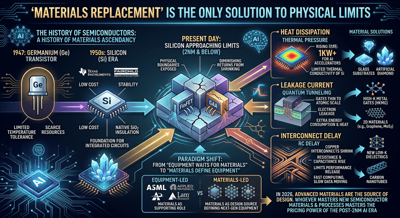
There is an old saying in the semiconductor industry: "One generation of materials, one generation of technology, one generation of industry." Viewed in the context of the AI computing power cycle in 2026, the weight of this saying is becoming even heavier.
In the past, the continuation of Moore's Law relied more on the advancement of manufacturing processes such as lithography, etching, and deposition. Today, as the process continues to advance to 2nm and below, simply relying on "more refined processes" has become increasingly difficult. Many problems can no longer be solved solely by equipment, but rather require returning to the materials themselves to find answers.
In other words, the history of semiconductors is also a history of materials continuously rising to prominence.
In 1947, the first transistor was made using germanium. Germanium played an important role in the early development of semiconductors, but its drawbacks were equally evident: insufficient temperature resistance, limited resource reserves, and difficulty in supporting large-scale industrial applications.
Entering the 1950s, companies represented by Texas Instruments and Fairchild Semiconductor shifted to silicon. Silicon not only has low cost and good stability, but also can naturally form a silicon dioxide insulating layer. All this laid the foundation for the large-scale manufacturing of integrated circuits and opened the door to the silicon-based semiconductor era for the following decades.
If we say that in the past three decades, the industry has been meticulously carving on the material substrate of "silicon", then today, this substrate has been carved to near its limit.
As the line width continues to shrink and the structure continues to become more complex, the benefits are no longer linearly realized as they were in the past. The evolution from FinFET to GAA remains important, but structural innovation itself is also starting to approach a bottleneck.
Material innovation has thus been pushed back to the core position of the industry. As chip manufacturing processes approach 2nm, the physical boundaries of silicon will be exposed in a more direct way.
Heat dissipation is the first perceived pressure.
The power consumption of AI chips continues to rise, and high-end accelerators have already entered the kilowatt range. Silicon's thermal conductivity performance is limited in high-temperature environments, and heat tends to accumulate in areas with dense transistors. No matter how powerful the computing power is, if heat dissipation cannot keep up, it will be forced to downclock, and the performance release will naturally be compromised.
Leakage problems have also become more intractable.
When the gate insulator is as thin as only a few atomic scales, electrons no longer fully obey the rules of traditional circuits, but instead "tunnel through" via the quantum tunneling effect. This means that even when the chip is in a low-load state, it may still generate additional energy consumption and heat. Traditional silicon-based oxides have difficulty fully fulfilling the task of blocking electrons.
Interconnect delay is slowing down system efficiency.
Advanced chips have a large number of copper interconnect lines inside. As the size shrinks, resistance and capacitance increase simultaneously, and RC delay has become an important factor limiting performance release. Computing cores can operate faster, but data may not flow at the same speed. For AI chips, this contradiction of "fast computing but slow data transfer" will become increasingly prominent.
From "equipment and other materials" to "materials define equipment", this is an extremely important paradigm shift:
In the past, the semiconductor industry was more equipment-oriented. As long as equipment manufacturers such as ASML, Applied Materials, and Lam Research continued to improve their manufacturing capabilities, material companies mainly played a supporting role, providing higher-purity silicon wafers, photoresists, and chemicals.
Now, the problem has become more complex. To improve heat dissipation, the industry has begun to research new material paths such as glass substrates and artificial diamonds; to suppress leakage current, directions such as high-K metal gates and two-dimensional materials continue to receive attention; to adapt to High-NA EUV lithography, metal oxide photoresists are also accelerating verification.
By 2026, advanced materials will no longer be the "consumables" of manufacturing, but the "source" of design. Whoever masters the structure and process of new semiconductor materials will hold the pricing power in the AI era after 2nm.
Three types of advanced materials that change the competitive landscape
Looking at the semiconductor industry landscape in 2026, advanced materials are no longer a marginal discipline. It is influencing multiple high-growth sectors such as AI, electric vehicles, Data centers, and 6G communications.
From the perspective of industrial chain value, the most notable material opportunities can be roughly divided into three categories: advanced semiconductor materials, advanced lithography materials, and advanced packaging materials.
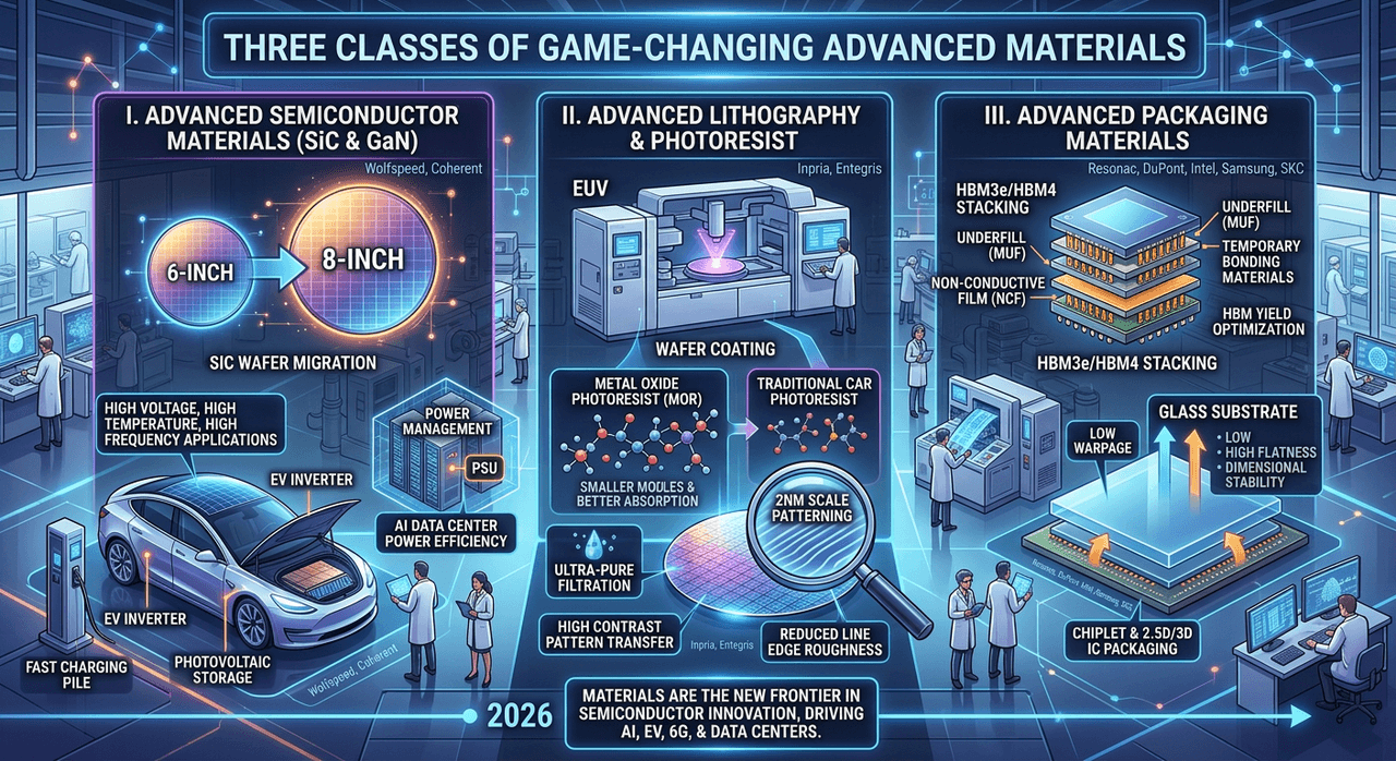
Third-generation semiconductor
If silicon is likened to a stable and mild traditional material, then silicon carbide and gallium nitride are more like hardcore materials capable of withstanding high-temperature, high-pressure, and high-frequency environments.
Their core value does not lie in replacing all silicon chips, but in entering scenarios where silicon is not good at: electric vehicle inverters, photovoltaic energy storage, industrial power supplies, data center power management, high-speed charging piles, etc.
Around 2026, the SiC industry is migrating from 6-inch to 8-inch wafers. Companies such as Wolfspeed and Coherent are all promoting the ramp-up of 8-inch production lines. If the yield rate and capacity release proceed smoothly, the unit cost is expected to continue to decline, and the market's concern about SiC being "too expensive" will also be partially alleviated.
The market once showed obvious concerns when Tesla proposed to reduce the SiC usage per vehicle. However, from an industrial perspective, this does not mean that the demand logic for SiC has been undermined. The decrease in SiC usage per vehicle often results from the improvement of system efficiency; meanwhile, the application scenarios of SiC are expanding from high-end electric vehicles to more energy conversion segments.
More importantly, AI Data centers are becoming new variables. As server power consumption rises, power management and energy conversion efficiency directly impact Data center operating costs. The advantages of SiC in high-voltage, high-temperature, and high-frequency scenarios give it strong strategic value in PSUs, ultra-fast charging piles, and industrial power grids.
Advanced Lithography and Photoresist
Lithography machines are often regarded as the core equipment for advanced semiconductor manufacturing processes, but photoresist also determines whether patterns can be accurately written onto wafers. If a lithography machine is a knife, photoresist is the material that receives the blade. As semiconductor manufacturing processes enter the 2nm scale, traditional photoresist is facing more and more challenges.
The pressure on traditional CAR photoresists is rising. Chemically amplified photoresists once supported multiple generations of advanced processes, but at extremely narrow linewidths, their molecular size, diffusion control, and pattern stability all face limitations. Line edge roughness, pattern collapse, and defect control all directly affect the yield of advanced processes.
Metal Oxide Resist (MOR) is emerging as an important candidate. MOR has a smaller molecular scale, stronger absorption capacity for EUV photons, and is more suitable for achieving high-contrast pattern transfer. Companies such as Inpria represent the R&D strength in this direction; Entegris provides key support in the areas of resist ultra-purification, transfer, and filtration.
Advanced packaging materials
When planar miniaturization hits a bottleneck, the semiconductor industry begins to seek answers in vertical space.
Chiplet, 2.5D packaging, 3D IC, and HBM stacking are becoming the mainstream paths for high-performance computing. The essence of advanced packaging is to compress more chips, higher bandwidth, and more complex interconnections into a limited space. Many of the most challenging aspects in this process fall on materials.
Glass substrates may become an important variable in the packaging system. Compared with traditional ABF substrates, glass substrates have lower warpage, higher flatness, and better dimensional stability. These characteristics are crucial for large-size AI packaging.
Enterprises such as Intel, Samsung, and SKC are all deploying glass substrates. If the relevant production lines enter the stage of actual mass production around 2026, glass substrates are expected to become one of the important directions for high-end AI chip packaging.
Specialized HBM materials directly impact yield. As the number of stacked layers in HBM3e and HBM4 continues to increase, 12-layer and 16-layer structures place extremely high demands on materials. Underfill adhesives, non-conductive adhesive films, temporary bonding materials, and electroplating chemicals must all maintain stability at extremely thin thicknesses while also avoiding bubbles, warping, and thermal mismatch.
Companies such as Resonac and DuPont have long been deeply involved in these niche segments. Although they may not be as prominent as memory manufacturers, they could directly impact the yield rate of HBM production, thereby affecting the profit distribution of the entire AI hardware supply chain.
In the field of advanced materials, the "verification period" itself is a competitive edge. Once a certain material enters the mass production list of leading customers such as TSMC, Samsung, and SK Hynix, it often accompanies multiple product generations. Investors should not only focus on short-term profits but also pay more attention to R&D directions and customer verification progress.
Those who are tackling 2nm MOR, advancing the glass substrate TGV process, and improving the yield of HBM materials will have a better chance of standing at the forefront of the next semiconductor cycle.
Core Leading Companies - The "Invisible Rulers" of Advanced Materials
In the view of the RockFlow Investment Research Team, in the semiconductor investment landscape of 2026, although some core leading companies do not directly sell chips, they control key consumables, formulas, and processes in advanced manufacturing processes and advanced packaging. Their value lies in the irreplaceability at the bottom of the supply chain.
Entegris (ENTG): The "Purification Gatekeeper" of Advanced Processes
In 2nm and more advanced manufacturing processes, the cleanliness requirements of the manufacturing environment have evolved from "clean rooms" to "atomic-level control". Even a single nanoscale metal impurity can potentially damage the transistor structure on a wafer. The core value of ENTG precisely stems from this extreme cleanliness requirement.
Filtration and purification are its most stable core businesses. Photoresist, electronic specialty gases, and ultrapure chemical liquids all require high-precision filtration during the process of transportation and use. As the manufacturing process continues to advance and the impurity tolerance continues to decline, wafer fabs will also raise their requirements for the performance, reliability, and replacement frequency of filters.
This means that ENTG's revenue not only follows the expansion of wafer production capacity but also benefits from the increase in the value of materials per wafer.
In addition, the precursor business of ENTG is highly correlated with advanced structures. In the atomic layer deposition process, special chemical precursors determine whether the thin film can "grow" uniformly and stably. After entering the GAA era, the transistor structure has become more complex, placing higher requirements on the molecular stability and reaction control of deposition materials.
ENTG's advantages in this stage enable it to not only be a consumables supplier but also gradually become a key participant in the advanced process system.
Embedded supply relationships bring high customer stickiness to ENTG. Wafer manufacturing is extremely cautious about material switching. Once TSMC, Intel, or Samsung determines the specifications of a set of filtration, chemical, or transmission systems during the R&D phase, they tend not to change them easily after mass production. This is because any replacement may introduce new defect risks.
This Path Dependence enables ENTG to have strong anti - cyclical capabilities.
Coherent (COHR): The "Master of Temperature Control and Transmission" Under Physical Limits
COHR is an electronic component company that is easily underestimated in computing power infrastructure. It is involved in SiC substrates and also deeply engaged in compound semiconductor materials such as InP and GaAs.
If the competition in AI chips focuses on computing power itself, then COHR addresses more two fundamental issues: how to efficiently convert energy and how to achieve high-speed data transmission.
SiC substrates are an important growth direction. COHR is one of the early manufacturers to promote the mass production of 8-inch SiC. As the industry migrates from 6-inch to 8-inch, whoever can steadily improve the yield rate will occupy a more favorable position on the cost curve.
Over the past few years, market attention on SiC has mainly focused on electric vehicles. However, from the perspective of 2026, AI Data centers, industrial power supplies, grid equipment, and charging infrastructure may become more resilient sources of demand.
Optical communication materials support the expansion of AI data centers. After the scale of AI clusters expands, the data transmission pressure between servers rises sharply. The increasing demand for 800G and 1.6T optical modules further enhances the importance of optoelectronic materials such as indium phosphide.
COHR has deep accumulation in material fields such as InP and GaAs, and its products directly affect the transmission efficiency, power consumption, and stability of optical modules. For Data centers, this is not a marginal requirement but an important component of system energy efficiency.
The diversified business structure enhances defensive attributes. Compared with companies more focused on SiC, COHR has multiple business fulcrums such as optical communications, industrial lasers, and material platforms. When SiC capacity expansion brings capital expenditure pressure, businesses such as optical communications can provide a certain amount of cash flow support.
This makes COHR more like a diversified materials platform rather than a single-category bet-type company.
DuPont (DD): The "Chemical Glue" in the Packaging Revolution
After Moore's Law slowed down in planar miniaturization, advanced packaging has become an important path to continue performance improvement. DuPont, with its long-term material accumulation, is regaining attention in 3D IC, HBM, and high-end packaging.
Its strength lies not in narrative, but in a large number of seemingly unremarkable yet irreplaceable material elements.
Advanced packaging requires stable bonding and insulating materials. In the multi-layer stacking of HBM3e and HBM4, not only stable connections need to be achieved between chip layers, but also thermal expansion, mechanical stress, and signal integrity need to be controlled. The polyimides, electroplating chemicals, and related electronic materials provided by DuPont have high technical barriers in these scenarios.
CMP polishing pads remain high-barrier consumables. In advanced processes, wafers need to be polished repeatedly to achieve a flatter surface and a more stable interlayer structure. The more complex the process, the more polishing steps are required, and the higher the value of related consumables.
DuPont is an important player in the global CMP polishing pad field, jointly forming a high-barrier supply pattern with companies such as CMC under Entegris. Its revenue is highly correlated with the "polishing area" and advanced process complexity in global wafer manufacturing.
Glass substrates open up a new window for materials.
If glass substrates accelerate commercialization in high-end AI packaging, DuPont's photosensitive materials, metallization processes, and TGV-related capabilities are expected to enter a new growth channel. For it, this is not a single product opportunity, but a structural opportunity brought about by the expansion of the advanced packaging materials system.
The purity of DuPont's electronic materials business is on the rise. As DuPont continues to divest non-core businesses, its electronic materials attributes have become more prominent. In the AI hardware cycle, material enterprises at the bottom of the supply chain tend to experience less revenue volatility and have relatively stronger order certainty. This makes DuPont a stable target that some institutional investors will focus on when allocating to the advanced materials theme.
Conclusion: Leading in advanced materials, it is expected to take over the pricing power of AI chips
RockFlow's investment research team believes that allocating to semiconductor advanced materials companies essentially means betting on the continued evolution of advanced processes and advanced packaging.
Regardless of how terminal chip design companies compete, as long as the manufacturing process continues to advance and packaging continues to upgrade, underlying materials such as filters, substrates, polishing pads, and packaging adhesives will still possess irreplaceable industrial value.
The winners in the materials industry are not necessarily the companies with the most active short-term stock prices. More often, they are the enterprises that quietly remain on the supply chain list and continuously increase their value in each generation of process upgrades.
In the semiconductor world beyond 2nm, competition occurs not only between chip architectures and manufacturing equipment but also within molecules, lattices, thin films, and interfaces. Cracks in silicon-based civilization are quietly emerging, and new pricing power is slowly growing from these cracks.
Related Content

Nokia's Revenge: From the Quagmire of 5G to AI and Optics, a Flash in the Pan or the Starting Point of a Long Bull Run?
Why Nokia is becoming one of the most hidden "beneficiaries of computing power" in 2026?

